OUR PROJECTS

UV Lithography Stepper
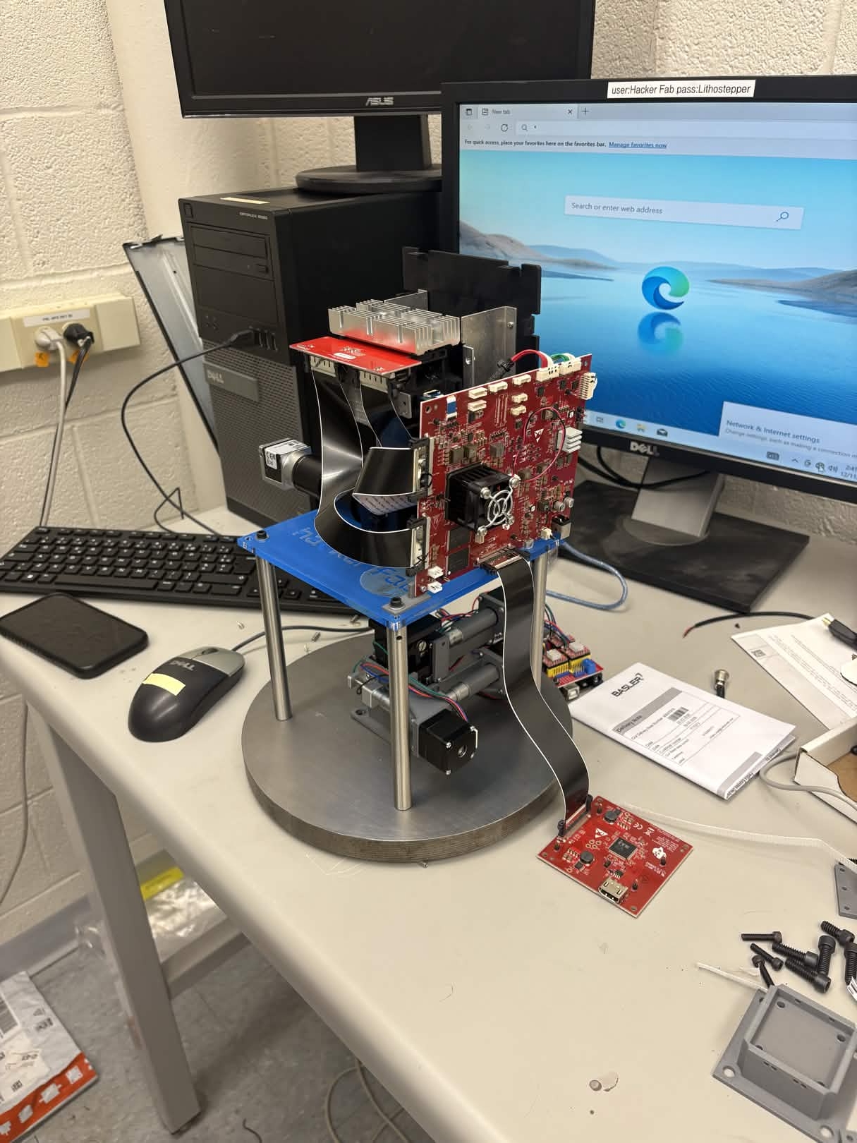
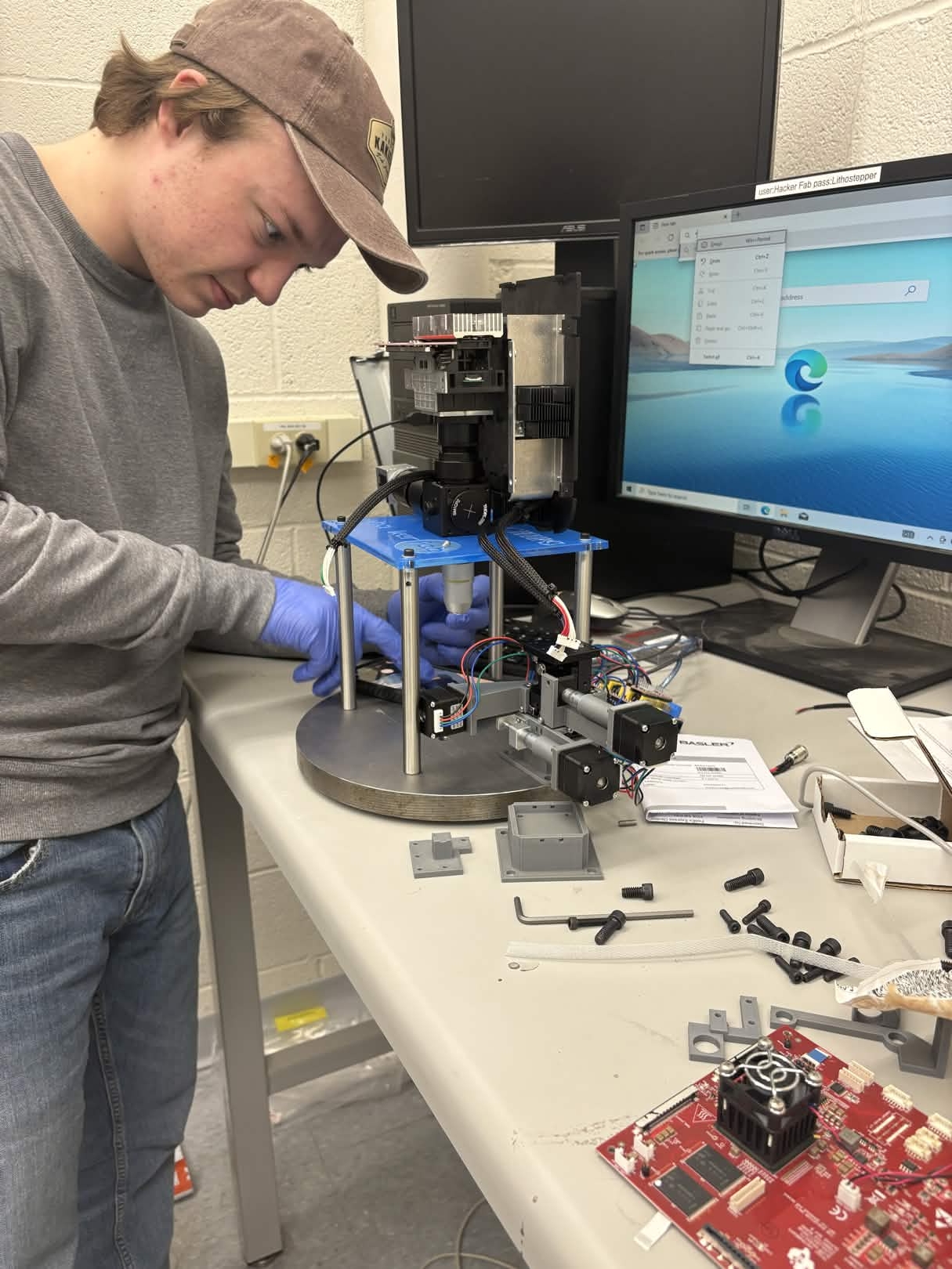
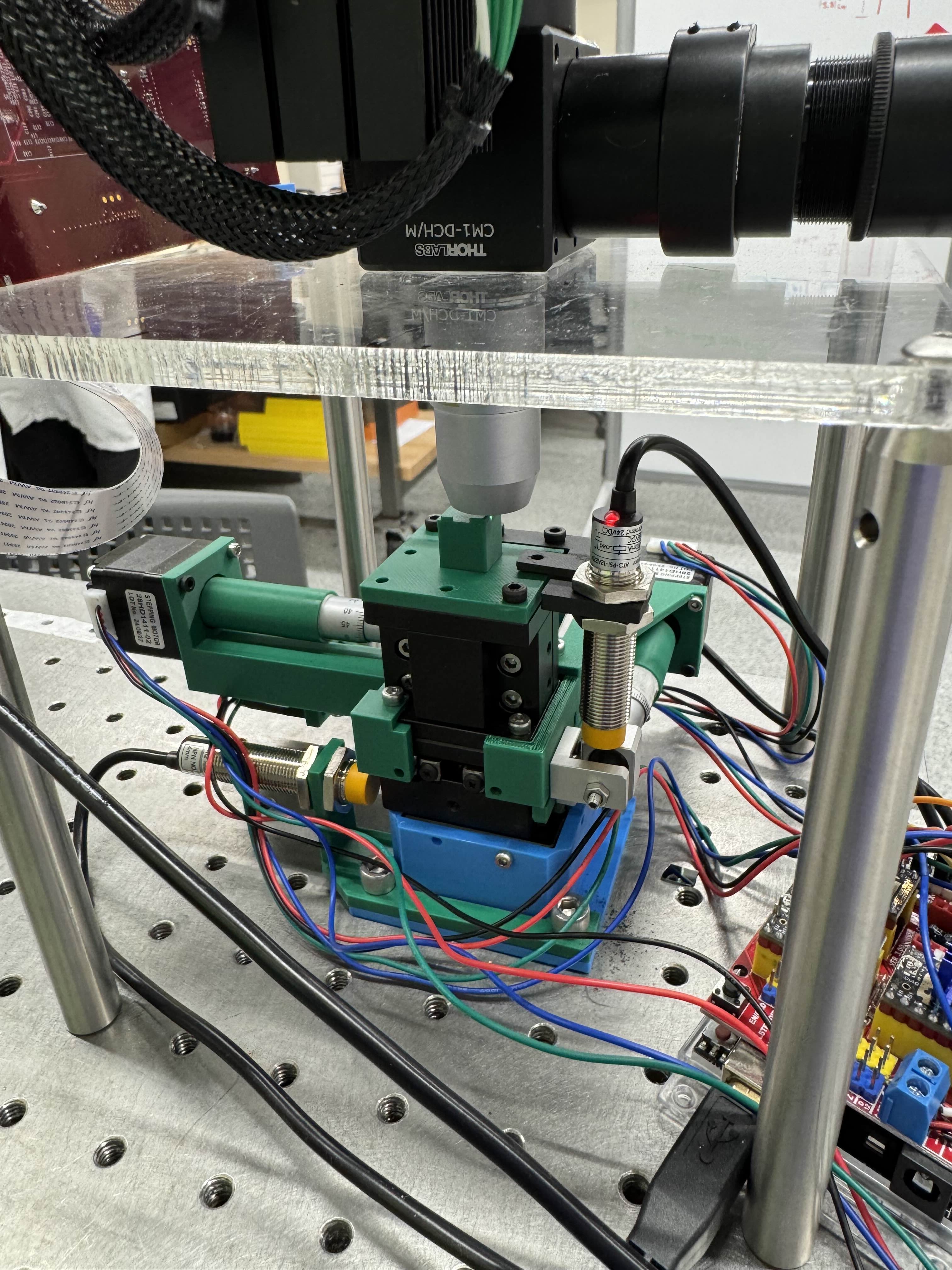
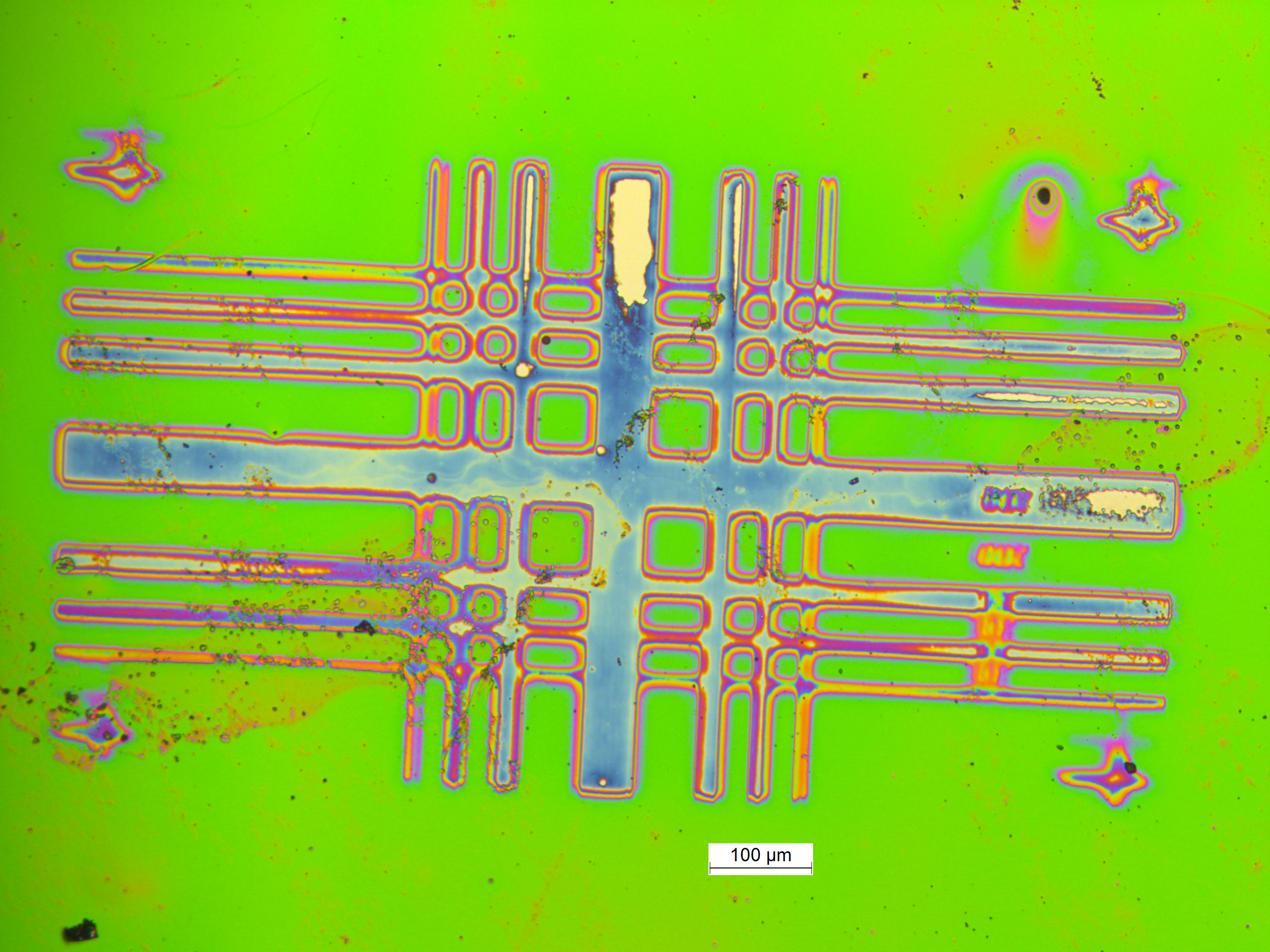
We're building a UV lithography stepper based on Carnegie Mellon's design. It uses a repurposed projector lens and a UV LED to expose photoresist through a chrome mask at roughly 2 micron resolution. Think[box] supported this build with $2,500 of funding.
Lithography is one of the core steps of semiconductor manufacturing. If you want to pattern features on a wafer, we need a reliable way to do it. This tool is an important part of the fabrication process.
We're looking for help with mechanical assembly, optical alignment, software, and process testing. No prior experience required; come to a build session and we'll help you get started.
Electroless Metal Plating
We're planning a wet chemistry station for depositing thin metal films on patterned surfaces through an autocatalytic reaction, without a vacuum or high voltages.
Metal contacts are a basic part of nearly every semiconductor device. Electroless plating lets us add metal to patterned wafers cheaply, while also giving members experience with surface chemistry and metallization.
This project is still being planned. If you're interested in chemistry, surface science, or materials processing, reach out via email or in person.
Thermal Evaporator
One of our longer-term goals is to build a thermal evaporator: a vacuum chamber that heats metal until it evaporates and deposits a thin film on the wafer. We'd use it for making aluminum and gold contacts on fabricated devices.
Clean metal contacts are essential for making chips that work. Thermal evaporation is a common way to produce better films than wet plating, and is the standard approach in research fabs. Building this would allow us to proceed to more advanced fabrication work.
This is still a future project, so getting involved now means helping with research, planning, and design. If you're interested in vacuum systems or thin-film processing, reach out via email or in person.

RF Sputtering System
This is one of our longer-term projects: an RF-powered vacuum system used to deposit thin films onto a wafer. Unlike thermal evaporation, sputtering can deposit insulators like silicon dioxide, which makes it important for our goal of fabricating a MOSFET transistor.
A MOSFET transistor needs a thin insulating gate oxide between the gate and the channel. Building the device to deposit that layer is a large step towards this goal.
This is still a future project, so getting involved now means helping with research, planning, and design. If you're interested in plasma physics, vacuum engineering, or dielectric materials, reach out via email or in person.